
2. Timing diagram 8085 | Memory Read
And here I have explained about the timing diagram of Memory Read Cycle.
Comments
Related Posts

4 Bit Serial Adder - Combinational Logic Circuit - Digital Circuits GATE

L-2.2: Implied Addressing Mode | Computer Organisation and Architecture

Front Office Executive Roles and Responsibilities In Hindi | Work Explained!
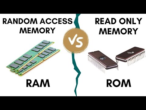
RAM vs ROM : Difference between them along with their types

micro operations introduction